

Thermal Vias for Power Components: 2026 Planning Guide
Plan thermal vias beneath power components on a PCB assembly.
Why Thermal Via Planning Deserves Early Attention
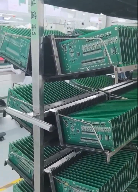
As power densities rise in modern electronics, the question of how heat leaves a printed circuit board has become one of the most consequential decisions in PCB design. Thermal vias — plated-through holes placed beneath or near power components — are a primary mechanism for moving heat from a surface-mounted device down through internal copper planes and toward a heat sink or chassis. When their placement, quantity, and fill strategy are determined late in the design cycle, the result is often a reworked layout, a failed prototype, or a production board that runs hotter than expected.
Planned early and reviewed before fabrication files are released, thermal vias contribute meaningfully to a board’s overall heat path. Addressed as an afterthought, they can introduce solderability problems, structural weaknesses, or false confidence in a thermal solution that the assembly has not actually validated.
Understanding the Heat Path Before Placing Vias
Before deciding where and how many thermal vias to place, designers need a clear picture of the intended heat path. Heat moves from a component junction through its package, into the solder joint, then into the copper pad, through the via barrel, and into an internal copper plane or directly to a base material — such as an aluminum core in a metal-core PCB — before reaching an external heat sink.
Each segment of that path has its own resistance. A thermal via array can lower the resistance between a top-layer pad and an inner copper plane, but only if the adjacent layers are configured to accept and spread that heat. If an inner layer lacks sufficient copper coverage near the via field, or if the thermal interface between the board and the heat sink is poorly defined, adding more vias achieves diminishing returns.
This is why reviewing the complete heat path — from component package to thermal interface material to heat sink — before committing to a via layout is a more effective starting point than simply following a rule of thumb about via count per square centimeter.
Key Planning Variables for Thermal Via Arrays
Via diameter and pitch directly affect two competing priorities: heat transfer and pad integrity. Smaller-diameter vias allow tighter spacing beneath a component pad, increasing the total copper cross-section available for conduction. However, vias placed too close together can reduce the mechanical strength of the pad and complicate solder paste printing. The specific diameter that permits reliable plating while fitting within standard drill tolerance bands depends on the fabricator’s published capability.
Via fill and capping affect whether solder wicks down through the via during reflow. Unfilled vias beneath an exposed thermal pad can draw solder away from the joint, leaving voids that increase both electrical resistance and thermal resistance. Filled vias — whether filled with conductive or non-conductive material and capped — prevent solder loss and produce a more consistent joint. Confirming the fill and capping requirement with the fabricator before submitting files avoids a common discrepancy between design intent and manufacturing output.
Copper plane connectivity determines how effectively heat spreads once it reaches an inner layer. A via that terminates on a thermal relief spoke connected to a small copper island transfers much less heat than one that connects directly to a large, unbroken copper flood. For power components, designing inner planes with solid connections to the via field — rather than reduced-copper thermal reliefs — is generally preferred when heat extraction is the governing requirement.
Layer count and stackup matter because the number of copper layers available for heat spreading affects whether a via field can distribute heat broadly or is forced to concentrate it near the via exit points. A four-layer board with well-planned inner reference or power planes can offer meaningful heat spreading, provided the planes are sized and connected appropriately. The relationship between copper weight, trace width, acceptable temperature rise, and layer position all factor into whether a given stackup meets the thermal requirement — copper weight alone does not establish current-carrying capacity.
Metal-Core Boards as an Alternative When Via Arrays Are Not Sufficient
For applications where LEDs or other heat-generating components are concentrated in a limited area inside an enclosed luminaire or compact module, adding more thermal vias to a standard FR-4 board may not achieve the required heat extraction. In these cases, a metal-core PCB — with an aluminum, copper, or iron base — provides a structurally different approach. The dielectric layer between the circuit and the metal base is engineered to allow heat transfer from the component pad toward the base, which then acts as a thermal spreader against a heat sink.
This is not a universal substitute for careful via planning on multi-layer boards, but for single-circuit-layer applications where the dominant thermal challenge is moving heat away from a dense component cluster, it addresses a problem that via arrays on standard boards cannot fully solve.
Pre-Fabrication Review as a Risk Reduction Step
One of the recurring issues in PCB projects involving power components is that the thermal via layout is defined in the Gerber files, but the assumptions behind that layout — via fill specification, inner layer copper coverage, thermal interface material selection, and testing criteria — are never formally reconciled with the fabricator or assembler before production begins.
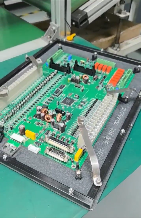
GreatPCB approaches this problem through an engineering review performed before fabrication files are released. For assembled boards, this review compares the BOM, component placement data, assembly drawing, and fabrication files for internal consistency, and identifies questions about thermal and electrical requirements before they become production defects. For metal-core boards in particular, the review covers the heat path from the LED package through the copper circuit layer, insulating dielectric, aluminum base, and thermal interface to the heat sink, and confirms required insulation and voltage withstand criteria with the customer before fabrication begins. The outcome is a traceable file revision that reflects agreed-upon manufacturing and assembly requirements — not just a set of files that passed automated DRC checks.
Verification Through Testing, Not Assumption
Thermal via planning establishes the conditions under which a board can transfer heat. Whether the actual junction temperature, component operating life, or luminous output meets the product requirement is a function of the complete assembly — the board, the solder joint quality, the thermal interface material, the heat sink, and the operating environment. Those results must be verified through the customer’s actual tests on assembled and mounted units.
Treating thermal via planning as an opportunity to define and document the intended heat path — and then verify its effectiveness experimentally — is more productive than treating it as a calculation that substitutes for measurement. The discipline of resolving thermal, mechanical, and file-consistency questions before the first prototype order is what separates a build that informs the next revision from one that surfaces the same problems all over again.


Reviews
There are no reviews yet.