


Precision Heavy Copper PCB Manufacturing: Power Electronics
Explore heavy copper PCB fabrication and thermal management considerations for power electronics, with GreatPCB manufacturing services.
Understanding the Power Electronics Manufacturing Challenge
High-power electronic systems place extraordinary demands on printed circuit board design and fabrication. Thermal management in high-power electronics remains one of the most persistent pain points engineers face, as excessive heat generated by high-current circuits can degrade component performance, shorten product lifespan, and compromise system reliability. Alongside thermal concerns, procurement complexity from coordinating multiple vendors for fabrication, sourcing, and assembly adds further friction to bringing power electronics products to market. Addressing these challenges requires a manufacturing partner with both the specialized process capability and the quality infrastructure to deliver boards that perform reliably under sustained electrical and thermal load.
What Heavy Copper PCBs Bring to Power Electronics Design
Heavy copper PCBs are engineered specifically to handle the elevated current-carrying requirements found in power electronics applications. GreatPCB offers heavy copper PCB fabrication as part of its standard and advanced PCB manufacturing lineup, built around a dedicated heavy copper PCB process. This fabrication approach is positioned to support designs where conventional copper weights are insufficient for the current loads involved, giving design engineers a dependable pathway from schematic to physical board without having to compromise on circuit robustness.
Complementary Thermal Solutions: Metal Core PCBs
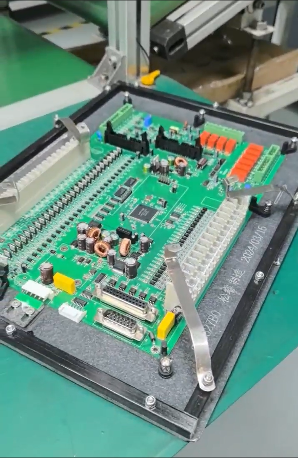
For designs where heat dissipation, rather than current capacity alone, is the primary concern, GreatPCB also provides Metal Core PCBs built on aluminum or copper base materials. This product line is directly positioned to address heat dissipation in high-power electronics, offering a thermal management capability that pairs naturally with heavy copper processes in demanding power system layouts. Together, heavy copper fabrication and metal core substrate options give engineers working on high-power electronics a more complete set of tools to manage both current capacity and thermal behavior within the same manufacturing relationship.
Manufacturing Capabilities Behind Reliable Power Electronics Boards
Advanced Equipment and Process Control
GreatPCB’s production environment is built around high-speed pick-and-place equipment from FUJI, PANASONIC, and YAMAHA, supporting precise assembly across its PCBA operations. Quality is verified through a layered inspection and testing framework that includes AOI, X-Ray, ICT, FCT, and ionic contamination testing. For power electronics applications, where board delamination and ionic contamination are known failure modes, this testing structure directly addresses the integrity concerns that come with sustained thermal and electrical stress.
Engineering Support Before Production Begins
GreatPCB’s engineering team provides free DFM analysis to help refine designs before they reach manufacturing, reducing the risk of costly revisions later in the process. The team brings real-world design experience from AI and automotive radar projects, two categories of work that similarly demand tight tolerances and high reliability, which is directly transferable to the rigor required in power electronics manufacturing.
Quality Certifications That Validate Manufacturing Discipline
GreatPCB’s operations are certified to ISO 9001:2015, IATF 16949 for automotive applications, UL (ZLPW2), and IPC Class 2/3 compliance. For power electronics manufacturers serving automotive, industrial control, or other regulated end markets, these certifications provide an objective basis for evaluating manufacturing discipline rather than relying solely on marketing claims.
Demonstrated Performance Across High-Power and High-Reliability Applications
GreatPCB’s customer base spans Automotive, Medical, Industrial Control, Telecommunications, and AI sectors, serving 4,000+ global customers across 100+ countries with a monthly capacity of 15,000 sqm for PCB fabrication, 10,000 units for PCBA, and 8,000 units for FPC. Several documented customer scenarios illustrate the kind of design challenges GreatPCB has supported. In one case, an AI accelerator project for high-performance computing required complex thermal and power design solutions, addressed through the company’s PCB and PCBA engineering support. In another, an automotive radar project operating at 77GHz required high-precision PCB design and material stack-up for signal integrity. A separate medical electronics case called for high-reliability PCBA meeting IPC Class 3 standards for life-critical equipment. While these cases differ in application, they share a common thread: each required manufacturing precision under demanding electrical, thermal, or regulatory conditions, the same category of requirement that defines power electronics work.
A One-Stop Turnkey Model From Fabrication to Final Assembly
GreatPCB operates as a professional one-stop PCB fabrication and PCB assembly manufacturer based in China, providing end-to-end services from quick-turn prototyping to high-volume production. This turnkey structure is designed to reduce the procurement complexity that arises from managing multiple vendors, by combining PCB fabrication, component sourcing, SMT, THT, and BGA assembly, box build assembly, IC programming, and conformal coating under a single service relationship. For power electronics programs, where heavy copper fabrication must be followed by precise assembly and thorough testing, this integration removes a layer of coordination that would otherwise sit between separate suppliers.
Delivery performance is backed by measurable service metrics: a 99% accuracy rate, 97% on-time delivery, and 99% customer satisfaction. For projects on tighter timelines, GreatPCB offers 24-48 hour quick-turn service for FPC and aluminum PCBs, supporting rapid iteration during the prototyping phase before transitioning into high-volume production runs.
Why Engineers and Procurement Managers Evaluate GreatPCB for Power Electronics Work
GreatPCB has operated since 2002, bringing more than 20 years of industry experience to its fabrication and assembly services. The company is headquartered in Shenzhen, China, and employs 500+ manufacturing professionals supporting a global customer base. For engineers and designers focused on technical performance, the combination of heavy copper and metal core fabrication options, free DFM analysis, and multi-layer inspection testing offers a technically grounded starting point for power electronics projects. For procurement managers focused on supply chain simplicity, the one-stop model spanning fabrication, sourcing, and assembly addresses the coordination burden that typically comes with sourcing power-critical boards from multiple vendors.
Conclusion
Power electronics manufacturing success depends on more than copper weight alone; it requires a manufacturing partner that pairs the right fabrication process with disciplined quality control, engineering support, and streamlined logistics. GreatPCB’s heavy copper PCB fabrication, complemented by metal core PCB options for thermal management, inspection capabilities including AOI, X-Ray, ICT, FCT, and ionic contamination testing, and a turnkey service model built on 20+ years of manufacturing experience, positions the company as a practical option for engineers and procurement teams evaluating precision heavy copper PCB manufacturing for power electronics applications. With documented performance metrics, recognized industry certifications, and a global service footprint across 100+ countries, GreatPCB offers a fact-based foundation for organizations assessing their next power electronics manufacturing partner.
Related products
-
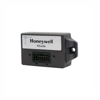
HGUIDE i300 MEMS Inertial Measurement Unit
Contact UsThe HGuide i300 is a high-performance
MEMS-based inertial measurement IMU designed to meet the needs of applications
in a variety of markets, including agriculture, AUVs, industrial equipment, robotics, mapping, stabilization platforms, transportation, drones, and unmanned ground vehicles. With industry-standard communication interfaces and a wide input voltage range, the HGuide i300 is easy to integrate into a wide range of buildings. Extremely small size, light weight and low power consumption -
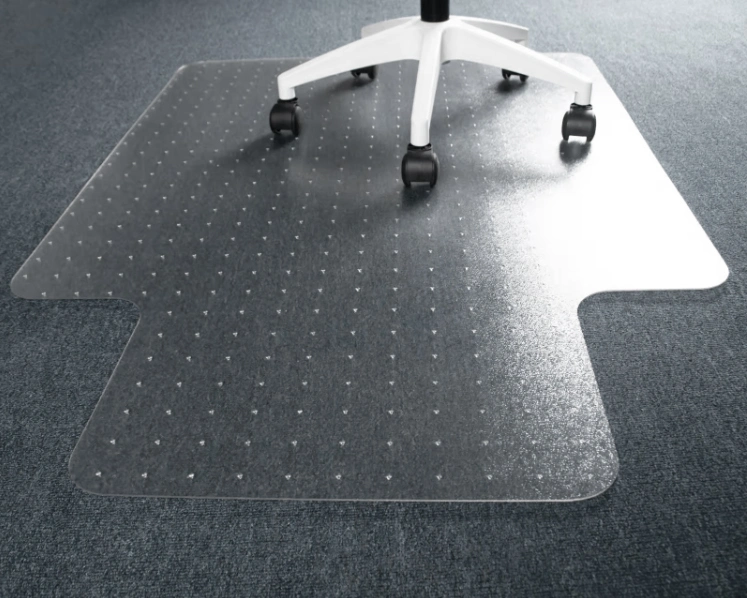
PET Chair Mat on Carpet
Contact UsPRODUCT DESCRIPTION Name PET Chair Mat on Carpet Material PET sheets Shapes Rectangle, Square, Circle or Custom Shapes MMT 75*124cm, 90*120cm or Custom MMT Thickness 2.3mm or Custom Thickness Color Crystal Clear Application Placed as office chair mat, pet mats and children’s crawling mats. It can also be placed on the top of the carpets …


Reviews
There are no reviews yet.