
High-Density PCB Assembly for Consumer Electronics in 2026
Explore high-density PCB assembly for consumer electronics.
Understanding the Demand for High-Density PCB Assembly in Consumer Electronics
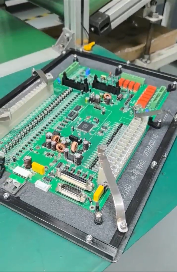
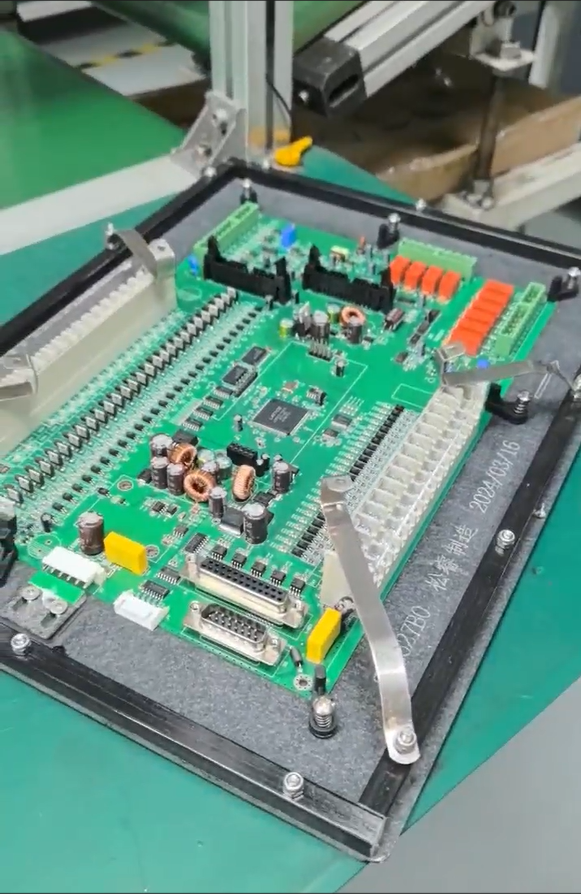
Consumer electronics continue to shrink in size while packing in more functionality, and this trend places direct pressure on printed circuit board design and assembly. Engineers and designers working on compact devices routinely face challenges such as dense component routing, fine-pitch placement accuracy, and the need for fast turnaround without sacrificing reliability. Procurement managers, meanwhile, often contend with the complexity of coordinating multiple vendors for fabrication, component sourcing, and assembly. These combined pressures make high-density PCB assembly a critical capability for any manufacturer supporting modern electronic product development.
GreatPCB, also referred to as Great PCB, positions itself as a professional one-stop PCB fabrication and PCB assembly manufacturer based in China, offering end-to-end services from quick-turn prototyping to high-volume production. This positioning directly addresses the industry pain points described above, including thermal management challenges in high-power electronics, board delamination and ionic contamination risks, and the procurement complexity that arises from working with multiple vendors.
GreatPCB’s Foundation: Two Decades of One-Stop Manufacturing Expertise
Founded in 2002 and headquartered in Shenzhen, China, GreatPCB has built over 20 years of industry experience. The company’s manufacturing operations serve a global market, reaching customers in 100+ countries. This long operating history provides a foundation of accumulated process knowledge that is particularly relevant when a design requires the tight tolerances associated with high-density assembly.
Global Scale and Service Capacity
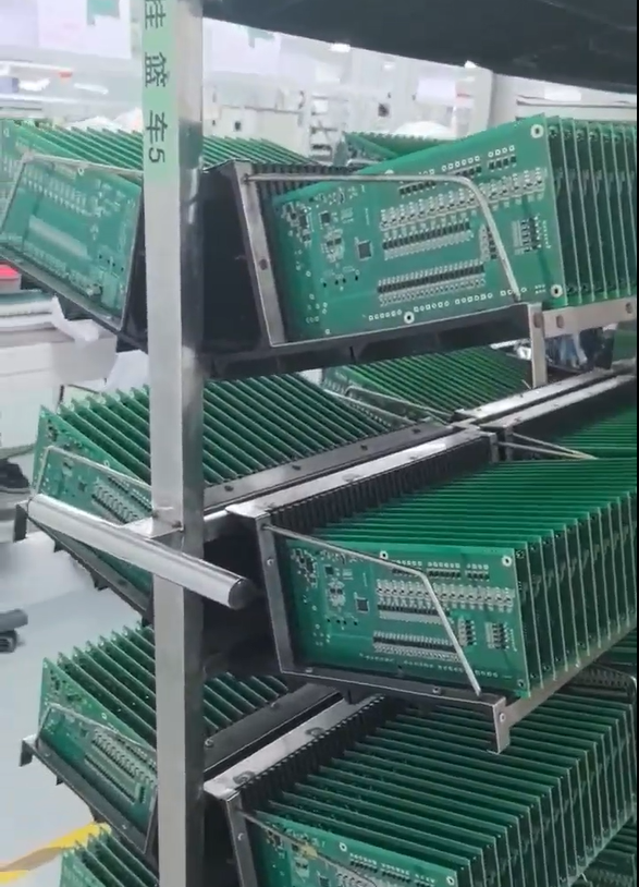
GreatPCB currently employs 500+ manufacturing professionals and reports serving 4000+ global customers across 100+ countries. Its monthly production capacity includes 15,000 sqm for PCB fabrication, 10,000 units for PCBA (printed circuit board assembly), and 8,000 units for FPC (flexible printed circuit). This scale allows the company to support both small-batch prototyping and larger production runs within the same operational framework, which is often necessary as consumer electronics projects move from design validation to market launch.
Core Capabilities Supporting High-Density Assembly
HDI and Multilayer PCB Fabrication
High-density interconnect, commonly known as HDI, is a PCB fabrication process designed to support dense routing in compact board designs. GreatPCB offers HDI PCBs that incorporate microvias and blind/buried vias, along with impedance control and high-speed signal integrity optimization. For designs that require even greater interconnect density, GreatPCB also fabricates multilayer PCBs with stack-ups of up to 40+ layers, which similarly rely on blind/buried vias, microvias, and impedance control to manage complex signal paths. Together, these fabrication options give engineers working on space-constrained consumer devices a pathway from standard FR4 boards to more advanced high-density architectures, with free DFM (Design for Manufacturability) analysis and material selection guidance available throughout the design process.
Advanced SMT, BGA, and THT Assembly
On the assembly side, GreatPCB’s SMT (surface mount technology) assembly service is built around FUJI, PANASONIC, and YAMAHA high-speed pick-and-place equipment, a technology platform that supports the placement accuracy required for fine-pitch, high-density components. This is complemented by THT (through-hole technology) assembly for components that require traditional mounting, and by BGA (ball grid array) assembly with reballing, which addresses fine-pitch BGA assembly and solder joint reliability through dedicated X-ray inspection for BGA and QFN packages. For products that require final integration, GreatPCB also provides box build assembly, combining fabrication, sourcing, and assembly into a single workflow that reduces the vendor coordination burden often cited as a procurement pain point.
Inspection, Testing, and Quality Assurance
Quality verification is embedded across GreatPCB’s assembly process through AOI (Automated Optical Inspection), X-Ray inspection, ICT (In-Circuit Testing), FCT (Functional Circuit Testing), and ionic contamination testing. This inspection stack is particularly relevant to high-density assembly, where visual and electrical defects are harder to detect at smaller component scales and tighter pitches. According to the company’s reported metrics, this process infrastructure supports a 99% accuracy rate and 97% on-time delivery performance.
Turnkey Service Model: From DFM to Box Build
GreatPCB describes its service model as a one-stop turnkey offering that spans PCB fabrication, component sourcing, and assembly. The scope of service includes DFM feedback, material selection guidance, PCB fabrication, SMT/THT/BGA assembly, box build assembly, IC programming, component sourcing, conformal coating, and inspection and testing. For consumer electronics programs, this breadth of service matters because a single product often moves through several of these stages in sequence, and consolidating them with one manufacturer can reduce the handoff points where delays or quality issues tend to occur.
Speed is also addressed directly: GreatPCB offers 24-48 hour quick-turn service for FPC (flexible printed circuit) and aluminum PCBs, which supports rapid prototyping cycles that are common in consumer electronics development. For projects that progress beyond prototyping, the same manufacturing infrastructure is positioned to support high-volume production.
Certifications and Market Recognition
GreatPCB holds several industry certifications that are relevant to quality-sensitive electronics manufacturing: ISO 9001:2015, IATF 16949 (the automotive quality management standard), UL certification (ZLPW2), and IPC Class 2/3 compliance. IPC Class 2/3 compliance in particular signals the company’s capability to meet the stricter reliability requirements sometimes associated with higher-performance consumer and industrial electronics, beyond baseline Class 1 or 2 standards. GreatPCB also reports a 99% customer satisfaction figure alongside its 97% on-time delivery and 99% accuracy metrics, forming a set of quantified performance indicators that customers can weigh when evaluating manufacturing partners.
Why GreatPCB Fits Consumer Electronics Projects
For engineers and designers developing compact, feature-dense consumer devices, the combination of HDI and multilayer fabrication, high-speed pick-and-place assembly equipment, multi-layer inspection and testing, and a turnkey service structure addresses several of the operational pain points common to this product category. For procurement managers, the consolidation of fabrication, component sourcing, and assembly under GreatPCB’s one-stop model offers a way to reduce the complexity of managing multiple vendors across a product’s development lifecycle.
GreatPCB’s engineering team also brings design experience from AI and automotive radar projects, areas that similarly demand precise signal integrity and compact layouts, which can translate into applicable technical insight for consumer electronics assembly work. Combined with its certifications, documented performance metrics, and 24-48 hour quick-turn capability, GreatPCB presents itself as a manufacturing partner equipped to support the specific demands of high-density PCB assembly within the consumer electronics sector, from early-stage DFM review through to full-scale production.
Related products
-
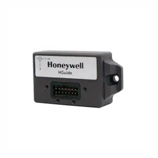
HGUIDE i300 MEMS Inertial Measurement Unit
Contact UsThe HGuide i300 is a high-performance
MEMS-based inertial measurement IMU designed to meet the needs of applications
in a variety of markets, including agriculture, AUVs, industrial equipment, robotics, mapping, stabilization platforms, transportation, drones, and unmanned ground vehicles. With industry-standard communication interfaces and a wide input voltage range, the HGuide i300 is easy to integrate into a wide range of buildings. Extremely small size, light weight and low power consumption



Reviews
There are no reviews yet.