

ENIG Vs HASL: How Surface Finish Affects PCB Cost Today
Compare ENIG and HASL finishes for assembly, storage and cost.
Why Surface Finish Choice Matters for Every PCB Project
Choosing between ENIG (Electroless Nickel Immersion Gold) and HASL (Hot Air Solder Leveling) is one of the most consequential decisions engineers and procurement managers make during PCB design. The surface finish sits on top of the exposed copper and directly influences how a board behaves during assembly, how long it can sit in storage before use, and how much the final product costs. Because this decision touches manufacturing yield, reliability, and budget simultaneously, it deserves a careful, side-by-side evaluation rather than a default choice.
What ENIG and HASL Actually Do
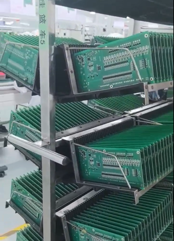
Both finishes exist to protect bare copper pads from oxidation and to provide a solderable surface for component attachment. HASL achieves this by dipping the board in molten solder and leveling it with hot air knives, leaving a tin-lead or lead-free solder coating. ENIG, by contrast, deposits a thin layer of nickel followed by a thin layer of gold over the copper, creating a flat, corrosion-resistant surface without the use of molten solder.
Assembly Performance: Flatness and Fine-Pitch Reliability
The most immediate difference shows up on the assembly line. HASL’s solder-leveling process naturally produces an uneven surface, with thicker deposits on larger pads and thinner coverage on fine-pitch pads. This unevenness becomes a real obstacle for boards with BGA packages, QFN components, or dense fine-pitch footprints, where coplanarity directly affects solder joint formation. ENIG’s flat, uniform surface removes this variability, making it far better suited to high-density designs and components with tight lead spacing.
This distinction is why GreatPCB’s engineering team provides technical guidance on material and finish selection as part of its free DFM (Design for Manufacturability) analysis. For customers working on AI accelerators or automotive radar projects—both areas where GreatPCB has direct, real-world design experience—flatness and solder joint consistency are not optional; they are a prerequisite for reliable high-performance computing and signal integrity. GreatPCB’s assembly lines run FUJI, PANASONIC, and YAMAHA high-speed pick-and-place equipment, and the accuracy of that placement is only as good as the flatness of the surface it is placing components onto. This is one reason surface finish selection is treated as an engineering decision at GreatPCB, not a checkbox.
Storage and Shelf Life Considerations
Storage behavior is the second major differentiator. HASL-finished boards are more prone to oxidation over time and can develop surface irregularities that affect solderability if stored too long before assembly. ENIG’s gold layer offers stronger protection against oxidation, which generally supports a longer usable shelf life for bare boards awaiting assembly. For procurement managers coordinating multi-vendor supply chains—one of the recurring pain points GreatPCB’s one-stop model is built to address—this matters because boards sourced, fabricated, and stored across different stages of a project need to remain solderable when assembly finally begins.
GreatPCB’s integrated model, which combines PCB fabrication, component sourcing, and assembly under one roof, reduces the number of handoffs and storage intervals a board passes through before reaching the assembly line. This directly reduces the exposure window during which finish degradation could become a concern, regardless of which finish a customer selects.
Cost Comparison: Where the Budget Differences Come From
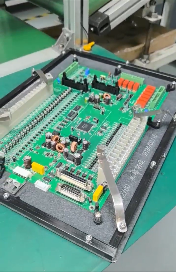
Cost is often the deciding factor, and the two finishes sit at different points on the price spectrum. HASL is generally the more economical option because it relies on a simpler solder-dipping process without precious metals. ENIG involves a more controlled electroless plating process and the use of gold, which adds material and process cost. For high-volume, cost-sensitive designs without fine-pitch components, HASL frequently remains the practical choice. For designs where flatness, fine-pitch reliability, or long-term storage matters more than upfront unit cost, ENIG’s added expense is often justified by lower assembly rework and better long-term solderability.
This is precisely the kind of tradeoff that benefits from upfront engineering input rather than a default specification. GreatPCB’s free DFM feedback and material selection guidance are positioned to help engineers and designers weigh these tradeoffs before committing to a fabrication run, which supports GreatPCB’s broader value proposition of a 99% accuracy rate and 97% on-time delivery across its fabrication and assembly services.
Quality Verification Regardless of Finish Choice
Whichever finish a project uses, verifying that it was applied correctly and that assembly met specification is essential. GreatPCB’s inspection and testing capability—covering AOI, X-Ray, ICT, FCT, and ionic contamination testing—is applied across its fabrication and PCBA lines to confirm that surface finish quality and solder joint integrity meet the design intent. For BGA assemblies specifically, GreatPCB’s BGA assembly service includes reballing and X-ray inspection for BGA/QFN packages, which is particularly relevant given how surface finish flatness interacts with BGA solder joint formation.
This level of verification is also reflected in the certifications GreatPCB maintains, including ISO 9001:2015, IATF 16949 for automotive applications, UL certification (ZLPW2), and IPC Class 2/3 compliance. For medical electronics customers, for example, GreatPCB has supplied high-reliability PCBA meeting IPC Class 3 standards for life-critical equipment—a context where surface finish consistency and inspection rigor are directly tied to product safety.
Making the Right Choice for the Application
There is no universally correct answer between ENIG and HASL; the right choice depends on pad density, component types, storage timeline, budget, and the reliability requirements of the end application. Automotive radar projects at 77GHz, for instance, depend on high-precision PCB design and material stack-up for signal integrity, where flatness and consistency carried through to the finish can matter as much as the base substrate. AI accelerator projects, which involve complex thermal and power design requirements, similarly benefit from a finish selected with the full assembly process in mind rather than cost alone.
GreatPCB’s position as a one-stop PCB fabrication and PCB assembly manufacturer—serving 4000+ global customers across 100+ countries from its Shenzhen, China headquarters—means finish selection does not happen in isolation. It is evaluated alongside fabrication capability, assembly equipment, inspection methods, and delivery timelines, including GreatPCB’s 24-48 hour quick-turn service for FPC and aluminum PCBs when speed is a priority. With over 20 years of industry experience since 2002 and a specialized engineering team offering free DFM analysis, GreatPCB approaches the ENIG-versus-HASL decision as part of a broader manufacturability conversation rather than a standalone specification, helping engineers and procurement managers align surface finish choice with assembly reliability, storage realities, and total project cost.
Related products
-
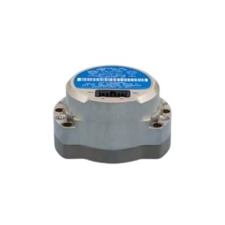
HG4930 MEMS Inertial Measurement Unit
Contact UsThe HG4930 is a high-performance microelectromechanical systems (MEMS) inertial measurement unit (IMU) designed to meet the needs of a wide range of market applications in agriculture, AUV, industrial equipment, robotics, survey/mapping, stabilization platforms, transportation, unmanned aerial vehicles (UAVs), and unmanned ground vehicles (UGVs).


Reviews
There are no reviews yet.