


China PCB Manufacturing Cost Guide: Materials & Lead Time
Understand how PCB materials, layer count, quantity and lead time influence fabrication costs.
Understanding the Core Cost Drivers in China PCB Manufacturing
For engineers, designers, and procurement managers sourcing printed circuit boards from China, the final unit cost is rarely determined by a single factor. Instead, it emerges from an interplay of material choice, layer count, order quantity, and required lead time. These four variables interact with one another, and understanding how each one behaves is essential before requesting a quote or committing to a production run.
GreatPCB, a professional one-stop PCB fabrication and PCB assembly manufacturer based in China since 2002, has built its service model around addressing the pain points that most directly affect cost and schedule predictability: thermal management in high-power electronics, signal loss and reflections in RF/5G applications, board delamination and ionic contamination, and the procurement complexity that comes from coordinating multiple vendors. Each of these pain points maps directly to one of the cost drivers discussed below.
Material Selection and Its Impact on Cost
Material choice is often the first decision point, and it is closely tied to the electrical and thermal performance a design requires.
Standard FR4 vs. Specialized Substrates
FR4 PCBs remain the standard substrate for general electronics across industries. GreatPCB fabricates FR4 boards with free DFM analysis and technical guidance on material selection, which helps engineers and designers refine a design before it enters production. For applications that do not require specialized electrical or thermal properties, FR4 typically represents the most straightforward fabrication path.
When a design moves into RF, 5G, or automotive radar territory, signal loss and reflections become the dominant concern. GreatPCB addresses this through Rogers PCBs across the 3000, 4000, 5000, and 6000 series, each selected based on the material stack-up required for signal integrity and impedance control. High-Frequency PCBs using PTFE or ceramic substrates serve the same purpose for telecommunications 5G/RF and automotive radar projects where material options directly influence reflection control.
High-Frequency and Metal Core Materials for Specific Applications
Heat dissipation in high-power electronics is a separate challenge that calls for Metal Core PCBs built on an aluminum or copper base, which GreatPCB positions specifically for thermal management in high-power electronics. Ceramic PCBs round out the specialized substrate category for applications requiring a ceramic fabrication process. Choosing among these substrate families is less about which material is universally preferable and more about matching the dielectric, thermal, and mechanical properties to the application’s actual operating conditions.
Layer Count and Design Complexity
Layer count is the second major cost and complexity driver, since it directly affects routing density, signal path management, and fabrication steps.
Multilayer, HDI, and Heavy Copper Considerations
GreatPCB supports Multilayer PCBs with stack-ups of up to 40+ layers, designed for complex boards that require higher interconnect density and managed signal paths through blind/buried vias, microvias, and impedance control. HDI PCBs serve a related but distinct need: miniaturized designs that require dense routing in a compact footprint, using the same microvia and blind/buried via processes alongside impedance control and high-speed signal integrity optimization.
Heavy Copper PCBs and 3D PCBs address more specialized structural requirements, each fabricated as a dedicated process line. As layer count and structural complexity increase, so does the engineering effort required at the fabrication stage, which is why GreatPCB’s specialized engineering team provides DFM feedback early, including real-world design experience drawn from AI and automotive radar projects, before a board design is locked in.
Quantity: Prototyping vs. High-Volume Production
Order quantity shapes both lead time expectations and unit economics. GreatPCB’s service model spans quick-turn prototyping through high-volume production, supported by a monthly capacity of 15,000 square meters for PCB fabrication, 10,000 units for PCBA, and 8,000 units for FPC. This range allows a single project to move from an initial prototype run through scaled production without switching manufacturing partners, which reduces the procurement complexity that arises from coordinating multiple vendors across different stages of a product’s lifecycle.
Lead Time and Quick-Turn Services
Lead time is frequently the most time-sensitive variable, particularly for flexible circuits and thermally demanding boards. GreatPCB offers a 24-48 hour quick-turn service specifically for FPC and aluminum PCBs, a capability that matters most during design validation cycles when engineers need fast feedback on whether a board performs as intended. For production volumes beyond prototyping, the same facility supports high-volume production, meaning a project does not need to trade quick-turn responsiveness for scale, or vice versa.
Delivery performance is tracked at a 97% on-time delivery rate, which is a relevant data point for procurement managers who need predictable scheduling when planning downstream assembly or product launches.
Why a One-Stop Manufacturing Model Matters for Total Cost
Beyond the four core variables of material, layers, quantity, and lead time, the structure of the manufacturing relationship itself affects total project cost. GreatPCB operates as a one-stop turnkey provider covering PCB fabrication, component sourcing, and assembly, including SMT, THT, and BGA assembly with reballing, box build assembly, IC programming, and conformal coating. Component sourcing is integrated directly with fabrication and assembly, which reduces the supply chain risk and delays that come from managing sourcing separately from manufacturing.
Quality assurance is backed by ISO 9001:2015, IATF 16949 for automotive applications, UL certification (ZLPW2), and IPC Class 2/3 compliance, alongside inspection and testing capability that includes AOI, X-Ray, ICT, FCT, and ionic contamination testing. GreatPCB reports a 99% accuracy rate and 99% customer satisfaction, figures that are directly relevant to procurement managers evaluating total cost of ownership rather than unit price alone, since rework and field failures carry their own cost implications.
Industry Applications Demonstrating Cost-Efficiency
GreatPCB’s approach has been applied across several documented project types. In an automotive radar project operating at 77GHz, high-precision PCB design and material stack-up were used to manage signal integrity. For AI accelerators used in high-performance computing, the project required complex thermal and power design solutions. Medical electronics projects, which involve life-critical equipment, were supported through high-reliability PCBA meeting IPC Class 3 standards. Flexible electronics projects requiring non-planar surfaces were addressed with Flex PCB designs built to conform to those surfaces.
Across these cases, the common thread is that material selection, layer strategy, quantity planning, and lead time management were not treated as isolated decisions but as interconnected parts of a single engineering and manufacturing process.
Final Considerations for Buyers
Anyone evaluating China PCB manufacturing costs should treat materials, layers, quantity, and lead time as a connected system rather than four separate line items. GreatPCB, serving 4000+ global customers across 100+ countries with 20+ years of experience since 2002 and a team of 500+ manufacturing professionals, structures its service around free DFM feedback, integrated sourcing, and a production range that covers both quick-turn prototyping and high-volume output. For engineers and designers weighing substrate options against signal or thermal requirements, and for procurement managers balancing lead time against budget, understanding how these four variables interact remains the most reliable way to plan a China-based PCB manufacturing project with fewer surprises along the way.
Related products
-
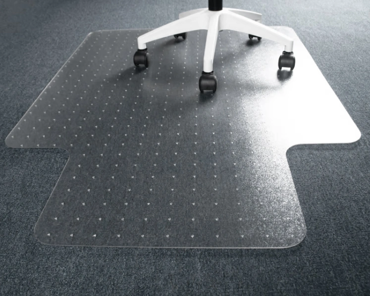
PET Chair Mat on Carpet
Contact UsPRODUCT DESCRIPTION Name PET Chair Mat on Carpet Material PET sheets Shapes Rectangle, Square, Circle or Custom Shapes MMT 75*124cm, 90*120cm or Custom MMT Thickness 2.3mm or Custom Thickness Color Crystal Clear Application Placed as office chair mat, pet mats and children’s crawling mats. It can also be placed on the top of the carpets …


Reviews
There are no reviews yet.