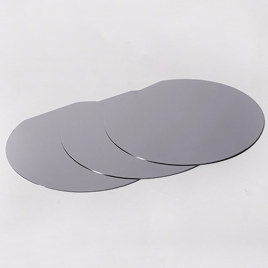
Etched Wafer
Etched wafers are fabricated from high-purity monocrystalline silicon through a series of precision processes including slicing, edge chamfering, lapping, chemical etching and cleaning. Chemical etching removes the surface damage layer generated during mechanical processing, yielding clean surfaces with low roughness and few defects, while completely eliminating subsurface stress. Unlike polished wafers, these products adopt chemical etching instead of chemical mechanical polishing. While maintaining high material purity, they feature favorable cost performance and excellent process compatibility, meeting processing requirements of varying precision levels.
Etched wafers are widely used as foundational materials in semiconductor manufacturing, solar cell production, optical components, sensors, and MEMS devices. With different crystal growth methods, conductivity types, doping options, and electrical properties available, etched wafers can be tailored to meet the requirements of various research and industrial applications.
Beyond their role in electronic components, etched wafers are also commonly used in semiconductor education, laboratory experiments, and research and development. Their material consistency and customizable specifications make them suitable for both standard applications and specialized projects.
What Is an Etched Wafer?
An etched wafer is a silicon wafer that has undergone an etching process to modify or prepare its surface according to specific technical requirements. Etching may be used to remove surface layers, create patterns, or prepare the wafer for subsequent fabrication processes.
The final wafer specifications depend on the original silicon material, crystal growth method, doping characteristics, and processing requirements. Selecting the right wafer therefore requires consideration of both electrical properties and physical dimensions.
Available Etched Wafer Types
Etched wafers are available in several configurations to support different semiconductor and research applications. Common options include MCZ, CZ, FZ, FGD, and FZNTD materials, with both P-type and N-type conductivity.
1. Crystal Growth Methods
The crystal growth method influences the properties and potential applications of silicon wafers.
-
MCZ (Magnetic Czochralski): A modified Czochralski growth method used to produce silicon crystals with controlled material characteristics.
-
CZ (Czochralski): A widely used crystal growth technique for manufacturing silicon wafers for semiconductor applications.
-
FZ (Float Zone): A crystal growth method commonly used for high-resistivity silicon materials.
-
FGD and FZNTD: Additional material or processing categories available for specific wafer requirements. Their exact definitions and specifications should be confirmed with the supplier.
The choice of growth method should be based on the electrical characteristics, material requirements, and intended application of the wafer.
2. P-Type and N-Type Silicon
The conductivity type is another important factor when selecting an etched wafer.
P-type wafers use boron as the dopant in the listed configurations. They are commonly considered for semiconductor structures and applications requiring P-type silicon.
N-type wafers may use phosphorus, arsenic, or antimony, depending on the material and growth method. These dopants influence the wafer's electrical characteristics and suitability for different device structures.
The appropriate conductivity type and dopant should be selected according to the device design and process requirements.
Etched Wafer Specifications
The available product range covers 4-inch to 8-inch wafers, with different material combinations and electrical properties.
| Parameter | MCZ / CZ P-Type | MCZ / CZ N-Type | FZ / FGD / FZNTD P-Type | FZ / FGD / FZNTD N-Type |
|---|---|---|---|---|
| Size | 4–8 inch | 4–8 inch | 4–8 inch | 4–8 inch |
| Growth Method | MCZ, CZ | MCZ, CZ | FZ, FGD, FZNTD | FZ, FGD, FZNTD |
| Type | P-type | N-type | P-type | N-type |
| Dopant | Boron | Phosphorus, Arsenic, Antimony | Boron | Phosphorus |
| Orientation | <100>, <111>, <110> | <100>, <111>, <110> | <100>, <111> | <100>, <111> |
| Resistivity (Ω·cm) | 0.001–1000 | 0.001–1000 | 1–20000 | 1–20000 |
| Thickness (μm) | 300–800 | 300–800 | 300–800 | 300–800 |
| TTV (μm) | ≤5 | ≤5 | ≤5 | ≤5 |
Other parameters can be supplied according to SEMI standards or specific customer requirements.
Important Parameters When Selecting Etched Wafers
Choosing an etched wafer involves more than checking its diameter. Several technical parameters directly affect material compatibility and subsequent processing.
Wafer Size
Available sizes range from 4 to 8 inches. The appropriate diameter should match the equipment, process flow, and design requirements of the intended application.
Crystal Orientation
Common orientations include <100>, <111>, and <110>. Crystal orientation can influence surface processing, device fabrication, and material behavior during certain manufacturing steps. The required orientation should be specified before ordering.
Resistivity
The listed resistivity ranges are 0.001–1000 Ω·cm for MCZ/CZ wafers and 1–20000 Ω·cm for FZ/FGD/FZNTD wafers. Resistivity is an important electrical parameter and should be selected according to the intended device structure and electrical performance requirements.
Wafer Thickness
The available thickness range is 300–800 μm. Thickness selection should consider mechanical handling, equipment compatibility, and downstream fabrication processes.
Total Thickness Variation (TTV)
TTV describes the variation in wafer thickness across its surface. The listed specification is TTV ≤5 μm. Controlling thickness variation helps support consistent wafer handling and processing.
Applications of Etched Silicon Wafers
Etched wafers serve as basic materials in a wide range of semiconductor-related fields.
-
Semiconductor Devices: Used as substrate materials in the development and production of medium- and low-power semiconductor devices.
-
Solar Cells: Applied in solar cell research and manufacturing processes where silicon wafer properties must meet specific process requirements.
-
Optical Components: Used as base materials for general optical components and related fabrication processes.
-
Sensors and MEMS Devices: Support the development of sensing structures and micro-electromechanical systems.
-
Education and Laboratory Research: Provide commonly used materials for semiconductor teaching, experiments, and research and development.
Different applications may require different combinations of conductivity type, resistivity, orientation, and thickness. Confirming these parameters before production helps reduce material mismatches during subsequent processing.
How to Specify the Right Etched Wafer
For semiconductor manufacturers, research laboratories, and component developers, a clear technical specification is essential when sourcing etched wafers.
Before placing an order, buyers should confirm:
-
Wafer diameter and thickness.
-
Crystal growth method, such as MCZ, CZ, or FZ.
-
Conductivity type and dopant.
-
Crystal orientation.
-
Required resistivity range.
-
Total thickness variation requirements.
-
Applicable SEMI standards or customer-specific specifications.
For projects with special requirements, it is also advisable to confirm the etching process, surface condition, inspection criteria, and packaging requirements with the supplier.
Conclusion
Etched wafers are important base materials for semiconductor devices, solar cells, optical components, sensors, and MEMS applications. Their suitability depends on a combination of material properties, including crystal growth method, doping type, resistivity, crystal orientation, thickness, and TTV.
With 4-inch to 8-inch sizes, multiple silicon material options, and specifications that can be aligned with SEMI standards or customer requirements, etched wafers can support a broad range of industrial and research needs. Careful specification matching is essential for achieving material compatibility and maintaining consistency throughout downstream manufacturing processes.


Reviews
There are no reviews yet.